NanoFlex Logo
THIS IS DAYLIGHT SAVINGS


Organic Photovoltaics
Changing The Landscape of Solar Power

Organic Photovoltaics are on the Rise

Organic electronics have gained rapid acceptance in the electronic display industry due to their low cost and ultra-thin, flexible form factor. Organic technology can also be applied to solar photovoltaics to completely redefine the way solar cells are fabricated and how and where solar power is used.

NanoFlex has developed the most extensive patent portfolio of small molecule organic photovoltaic, or OPV, technologies in the world. We believe that our intellectual property positions us as a gatekeeper for the future of the solar industry.

Organic Semiconductors Explained

Organic semiconductors are carbon-rich compounds with a structure tailored to optimize a particular function, such as responsiveness to a particular range of visible light. The use of organic compounds as semiconductors for commercial applications is relatively new. Organic semiconductors have elicited intense interest globally as they hold the promise of ultra-low cost and high performance along with a host of break-through new properties that unlock exciting new product opportunities in electronics, lighting, and photovoltaics.

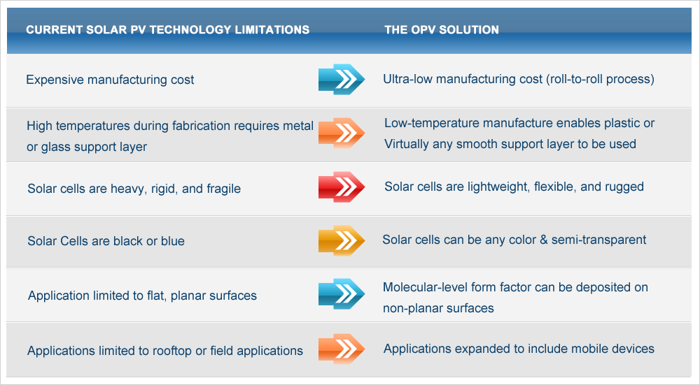
Organic photovoltaics offer a number of advantages ranging from rapid, ultra-low-cost manufacturing to extremely thin, lightweight, and flexible form factors, which present opportunities for revolutionary advances in the acceptance and deployment of solar energy. There is no restriction on the size and shape of OPV devices, and every conceivable shape and form can be envisioned, with only human synthetic capability as the limiting factor. The devices can be in the form of fibers, woven to fabrics, bent or rolled as films on curved surface. The near two-dimensional nature of OPVs will present a substantial paradigm shift and it may take some time before it is accepted by the mass market.

Check out the table below to see more advantages of OPVs.

 Table displaying the advantages of OPVs with current solar pv technology limitations on the left and the opv solution on the right.

Organic Photovoltaics is Altering the Course of Solar

A "small molecule” organic solar cell consists of very thin, nanometer-scale organic active layers sandwiched between two electrodes – a transparent anode and a metallic cathode. Typically, the anode is an optically transparent conductive metal oxide layer that lets light enter the device for absorption within the active layers. Low work-function metals (such as magnesium, aluminum, silver, and their alloys) are commonly used as cathodes. There is no restriction on the size and shape of OPV devices, thus every conceivable shape and form can be envisioned. The devices can be in the form of fibers, woven into fabrics, bent, or rolled as films on curved surface. The near two-dimensional nature of OPVs represents a new paradigm shift in solar industry.


Video thumbnail image. Play icon on top of rectangles and lines displaying the inner workings of an organic cell.

Play the video to see the inner workings of an organic solar cell.

Fundamental Principles of OPV operation

An organic solar cell consists of nanometer-thin organic layers sandwiched between two electrodes. The basic mechanism of photocurrent generation in OPVs can be illustrated with two organic materials, one a net electron donor (D) and the other an acceptor (A).


Call out  Light Absorption

The first step of the process is light absorption, leading to exciton formation. The exciton can be formed in either the donor or acceptor layer. In order to cover a large fraction of the solar spectrum, the donor and acceptor materials chosen for OPVs have broad absorbance lines and high extinction coefficients, giving a high optical density for thin films.


Call out  Exciton Diffusion

Once formed, the exciton then migrates to the D/A interface,
or alternatively decays to the ground state. Materials and film
thicknesses are carefully selected to maximize the yield of excitons
that reach the D/A interface.


Call out  Charge Separation

At the D/A interface the exciton undergoes a charge transfer reaction, forming a hole and electron in the D and A layers, respectively. In this process an electron is transferred from the donor to the acceptor, in an exothermic process. The optimal choice of a pair of D/A materials is one which gives efficient exciton charge separation, but maintains a large energy difference between the donor hole and acceptor electron to keep a high open cell voltage.


Call out  Charge Transport & Collection

After the hole and electron are generated, they are conducted through the D and A materials and extracted by the electrodes (charge collection). Once charges reach the electrode and are extracted and transferred to the outer circuit, the electron is transferred to the cathode and the hole to the anode.


NanoFlex's OPV Technology Platform

NanoFlex's OPV technology platform is based on flexible, thin-film organic technologies that it has researched and developed over the last two decades. NanoFlex's approach has been to advance all dimensions of OPV technology, including the development of new materials (some of which are now being sold in small quantities by materials suppliers), new high efficiency device architectures, and ultra-high-speed, energy efficient production processes such as organic vapor phase deposition developed in our research partner's laboratories, and solar cell modulization.

OPV Technology Platform

Contact us today to learn more!

           
Home About Us Technology Applications Investor Relations Contact Us
           
space
THIS IS DAYLIGHT SAVINGS
space